"Opening the Era of 1,000 Tokens per Second"…Samsung Electronics Drives AI Semiconductor Innovation with zHBM
3D Stacked Architecture Unveiled at U.S. AI Infrastructure Summit
Eight Times the Performance and Three Times the Power Efficiency Compared to HBM5
Samsung Electronics has unveiled “zHBM,” a memory stacked directly in 3D on top of AI accelerators, signaling its vision to boost the response speed of existing AI systems by more than tenfold in the era of artificial intelligence (AI) agents.
Kim Indong, Executive Director for Memory Product Planning at Samsung Electronics America Corporation (DSA), emphasized the paradigm shift in AI memory semiconductors during his keynote address at the AI Infrastructure Summit held at the Santa Clara Convention Center in California, USA, on September 16 (local time).

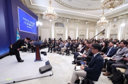
Kim Indong, Executive Vice President in charge of Memory Product Planning at Samsung Electronics America (DSA), is giving a presentation at the "AI Infrastructure Summit" held on the 16th (local time) at the Santa Clara Convention Center in California, USA. Photo by Yonhap News
View original imageExecutive Director Kim stated, “The current response speed of conversational AI systems is limited to around 100 tokens per second per user,” and added, “We are aiming for a quantum leap to raise this figure to 1,000 tokens per second in anticipation of the coming era of agent-based AI.”
To enable this dramatic performance improvement, the core breakthrough suggested by Samsung Electronics is “zHBM.” Whereas the industry currently adopts a 2.5D packaging approach where high bandwidth memory (HBM) is placed flat alongside AI accelerators, this results in bottlenecks due to data transmission distances and pathway limitations. Samsung intends to completely overcome these limitations by implementing a 3D structure, vertically stacking HBM directly on top of the accelerator.
Executive Director Kim compared this to “installing a dedicated elevator that takes guests straight from their hotel room to the lobby,” explaining that data transfer distances and resulting bottleneck-induced delays can be drastically reduced. As a result, zHBM can deliver up to eight times the performance and more than three times the power efficiency compared to HBM5. Samsung also plans to address the challenge of heat transfer from the accelerator during vertical stacking through a collaborative design system, involving custom solutions in cooperation with AI accelerator clients from the initial product design stages.
In addition, Samsung Electronics revealed a roadmap for “zNAND-O,” a NAND flash-based 3D storage solution targeting the on-device AI market.
Executive Director Kim stated, “By 2030, it will become common to run giant AI models with one trillion parameters even on environments such as AI workstations, rather than just large-scale servers. While configuring memory for one trillion parameters with only DRAM would be extremely costly, the application of zNAND-O can achieve this at just one-sixth of the cost.”
Hot Picks Today
 Seoul Tops London and Tokyo for the First Time... Foreign Media: "Seoul Is Becoming the New Paris"
- "Where Is My Suitcase?" 26 Checked Bags Missing at Incheon Airport in 10 Days... Why?
- Just Two Days After Release, iPhone 18 Pro Users Worldwide Report Sudden Reboots and "Panic Full" Issues
- "Is the YouTuber Telling the Truth?" 300,000 Views in One Day... The Real Story Behind Shin Ramyun's Flavor, According to Nongshim [Tastelovers X-File]
Samsung Electronics plans to begin full-scale sample supply of zNAND-O to clients starting in 2028. Executive Director Kim further added, “We are confident that we will deliver unparalleled value to our clients in terms of ‘time to market,’ which is the core of competition in AI semiconductors.”
© The Asia Business Daily. All rights reserved. Unauthorized AI training and use prohibited.