Sony and TSMC to Begin Mass Production of Next-Generation Image Sensors in Kumamoto, Investing 1 Trillion Yen
Japan's Sony and Taiwan's TSMC plan to invest approximately 1 trillion yen to begin mass production of next-generation semiconductors for image sensors as early as 2029 in Kumamoto Prefecture, Japan.

On August 10, the Nihon Keizai Shimbun (Nikkei) reported that the two companies are expected to reach an agreement on mass production investment soon and establish a joint venture within fiscal year 2026. In May, Sony and TSMC signed a memorandum of understanding (MOU) to establish a joint venture for the development and production of next-generation image sensors.
The joint venture plans to build large-scale development facilities and production lines at the image sensor plant owned by Sony Semiconductor Solutions in Koshi City, Kumamoto Prefecture. They aim to begin mass production in 2029, about three years from now. Sony is expected to contribute approximately 60% of the investment, while TSMC will provide about 40%. Nikkei predicts that the total investment will amount to around 1 trillion yen, equivalent to about four years of capital investment in Sony's semiconductor division.
The joint venture is expected to supply high-performance camera sensors for Apple iPhones. In the future, the companies plan to improve sensor performance to enhance AI recognition accuracy, thereby expanding applications into the field of "physical AI" where artificial intelligence directly controls robots, automobiles, and other physical devices.
Sony holds more than half of the global market share in the complementary metal-oxide semiconductor (CMOS) image sensor market. With China-based OmniVision and Samsung Electronics rapidly investing to catch up, Nikkei points out that Sony's strategy is to further widen the technological gap with competitors by partnering with TSMC, which is a leader in advanced semiconductor technology.

Until now, Sony has directly developed and mass-produced image sensors, while outsourcing production of the processing semiconductors to TSMC—a model of divided work. Moving forward, the two companies plan to expand their collaboration to joint production through the new joint venture, aiming to respond to increasing demand for image sensors driven by the expansion of AI.
However, it is reported that Sony does not intend to disclose to TSMC the core manufacturing technologies of image sensors in which it holds a competitive advantage. By expanding its partnership with Sony, the world's largest image sensor company, TSMC will accumulate related technology and know-how. Through this, TSMC aims to enhance its competitiveness in the physical AI sector.
Hot Picks Today
 "Visited Three Clinics, Still Told to Wait an Hour"... The Sigh of a Grandmother Unfamiliar with Apps
- [Exclusive] Why Are Turnovers So High? "A 10 Million Won Base Salary Gap at the Same Workplace" [National Pension Staff Shortage]②
- [Exclusive] "Is Bureaucratic Discretion Above the Law?" Application Denied at One Word...Will This 68-Year-Old Law Finally Change?
- "Startled Awake from a Nap" Giant Signboard Crashes Beside Head... Chinese Man Survives Miraculously
- "I Thought Everyone Was Heading to Japan"... The Top Overseas Travel Destination for Chuseok Was This Unexpected Country
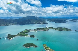
Kumamoto Prefecture is well-suited for semiconductor production thanks to its abundance of water resources and easy access to inexpensive electricity generated by geothermal and solar power as renewable energy sources. Sony and TSMC also plan to continue investing in semiconductor production in Kumamoto Prefecture over the long term.
© The Asia Business Daily. All rights reserved. Unauthorized AI training and use prohibited.
![Even With 400 Million Won in Net Assets, Not Middle Class... 6 Criteria That Define the "True Middle Class" [Data Pick]](https://cwcontent.asiae.co.kr/asiaresize/307/2026092809144741876_1790554486.jpg)