Samsung Redraws Its ‘National Production Map’… But Is It Feasible? [Why&Next]
Transition to Next-Generation Fields at Nationwide Production Sites
Focusing on HBM, OLED, and Physical AI Lines
"Securing Market Demand" May Be Applied in Stages
In line with the government's regional balanced investment initiative, Samsung is restructuring its domestic production map. While maintaining its existing semiconductor production system centered in the Seoul metropolitan area, the company plans to allocate next-generation semiconductor, display, and physical artificial intelligence (AI) manufacturing functions to the Chungcheong, Honam, and Yeongnam regions. Industry insiders note that now is the time for a technological shift to meet demand in next-generation sectors, and that this transformation is already underway. However, there remains the challenge of whether large-scale regional investments worth hundreds of trillions of won can be realized as planned, especially considering that even the Yongin Semiconductor Cluster has yet to fully break ground.
Samsung has recently unveiled a plan to restructure the roles of its major domestic business sites in line with the government’s nationwide advanced industry investment initiative. Currently, Samsung's domestic production bases include semiconductor front-end facilities in Giheung, Hwaseong, and Pyeongtaek under Samsung Electronics; back-end and advanced packaging hubs in Onyang and Cheonan; display production centers in Giheung, Asan, and Cheonan under Samsung Display; battery and electronic materials facilities in Cheonan, Ulsan, Cheongju, and Gumi under Samsung SDI; and the mobile manufacturing hub in Gumi under Samsung Electronics.
The core of this new plan is for Samsung Electronics, as an integrated device manufacturer (IDM), to expand its nationwide production facilities with a focus on next-generation semiconductor and AI manufacturing capabilities. Out of its long-term investment plan totaling 2,655 trillion won, Samsung has allocated 2,030 trillion won to semiconductor hubs in the metropolitan area such as Pyeongtaek and Yongin, and 625 trillion won to non-metropolitan regions including Honam, Chungcheong, and Yeongnam. While maintaining the existing metropolitan-centered semiconductor production system, the company will enhance each region with additional functions such as high bandwidth memory (HBM), next-generation displays, and physical AI manufacturing.
![Samsung Redraws Its ‘National Production Map’… But Is It Feasible? [Why&Next]](http://www.asiae.co.kr/news/img_view.htm?img=2026070310551633279_1783043717.jpg)
The first area expected to see a shift in roles is the Chungcheong region. Onyang and Cheonan in South Chungcheong Province have already served as key hubs for Samsung Electronics’ semiconductor back-end processing and advanced packaging. With the rising demand for AI semiconductors and the increasing importance of HBM, this region is expected to emerge as a back-end hub, completing HBM through packaging and testing after memory production. Pyeongtaek will focus on front-end processes such as wafer production, while Cheonan and Onyang will strengthen the production system that enhances HBM quality.
The Honam region is being considered as the candidate site for Samsung’s next semiconductor fabrication plant. The company is open to the possibility of building new semiconductor production facilities centered around Gwangju. The long-term vision is to extend the currently metropolitan-focused semiconductor front-end bases into the Honam region. If implemented, Samsung’s semiconductor production map would shift from a structure concentrated in southern Gyeonggi Province to one where metropolitan front-end facilities are connected with advanced manufacturing hubs in various regions.
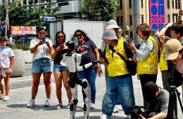
In Yeongnam, Gumi is set to be transformed into a physical AI stronghold. The Gumi business site has functioned as Samsung Electronics’ mobile manufacturing hub, but given the declining profitability of the mobile sector, the company appears to be preparing for future industries. Going forward, the site is expected to leverage its existing manufacturing base to enhance production capabilities in physical AI fields such as robotics, AI devices, and digital twins. On June 29, Samsung Electronics announced via public disclosure that it would build a “humanoid robot line” in Gumi, with a high likelihood of utilizing idle land within Gumi Plant 1 and 2. However, since physical AI remains an unproven domain in terms of large-scale productivity and profitability in Korea, investing in non-metropolitan regions carries considerable risk.

The key factor for Samsung Display’s investment in the Chungcheong region is also demand. Samsung Display has announced plans to develop the Cheonan and Asan area into a next-generation OLED cluster. The target is to expand OLED demand beyond smartphones to include automotive, laptop, tablet, and other IT and electronic applications. The display industry expects sufficient demand. As OLED demand—currently supplied almost entirely by domestic companies—grows rapidly, both Samsung Display and LG Display are accelerating production line expansions. However, because the display industry is sensitive to economic fluctuations and downstream demand, sustained large-scale facility investments will require mid-to-long-term demand growth as a prerequisite.
Industry observers believe this initiative is significant in that it expands Samsung’s domestic production base nationwide. Until now, Samsung’s semiconductor investments have been concentrated in the southern Gyeonggi Province areas of Giheung, Hwaseong, and Pyeongtaek. The new plan connects the Chungcheong HBM back-end hub, the next fab in Honam, and the physical AI manufacturing base in Yeongnam, aiming to shift from a “metropolitan area-centric semiconductor map” to one where metropolitan front-end facilities are linked with regional AI manufacturing hubs.
However, feasibility is a separate issue. With semiconductor plant construction in the Yongin Semiconductor Cluster yet to be fully underway, simultaneously advancing large-scale investments in the Honam, Chungcheong, and Yeongnam regions requires resolving complex issues such as electricity supply, water resources, land acquisition, workforce, and regulatory approvals. From groundbreaking to completion and mass production stabilization, semiconductor fabs require a lengthy timeline and capital investments on the scale of tens of trillions of won. For example, the Samsung Electronics fab in the Yongin National Industrial Complex, targeting initial operation in the second half of 2030, is already delayed due to postponed site development bids.
There is also the possibility of a gap emerging between the government’s regional balance strategy and corporate investment decisions. For companies, market demand and profitability inevitably take precedence over the policy rationale of regional balance. In fact, Samsung’s investment plans are focused on sectors expected to see future market growth, such as AI semiconductors, HBM, OLED, and physical AI. Even if the government designates regional hubs, actual investments may be implemented in phases depending on market conditions. An industry source commented, “In the case of the Chungcheong region, land, power, and water are all prepared, and it appears that feasibility and investment value have already been analyzed in advance. In contrast, whether Honam investments will actually be executed remains uncertain.”
Hot Picks Today
 "Even If SK hynix Stock Falls to Zero, I Won't Sell" "Korean Market Is Too Risky" U.S. Retail Investors Panic Amid Plunge
- [Exclusive] "Requesting Severe Punishment"... Lee Eonju Files Police Complaint Against Executive for Distributing Lewd Composite Images
- In This Place Where 150,000 Won Is Given Monthly Per Person... 90% of the Funds Were Actually Spent
- "Expected an Idol Look, but Why Is This 200 Million Won Robot Like This?" Flood of Complaints Leads to Discount Coupons
- Spraying Water Once Costs 2.26 Million Won... Chinese Apartment Complex Tackles Heatwave with 'Rooftop Rain'
Park Jaekun, president of the Korea Society of Semiconductor and Display Technology, stated, “Samsung invests based on market prospects. For displays, the automotive and laptop OLED markets are growing, and the company appears to be trying to secure demand leadership. It will take time, but without preparation, there is no future.”
© The Asia Business Daily. All rights reserved. Unauthorized AI training and use prohibited.