SK hynix to Invest 100 Trillion Won in Cheongju to Strengthen NAND and Packaging Hub
SK hynix is making a total investment of 100 trillion won in semiconductors in Cheongju, Chungcheong region.
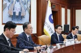
On July 2, Nojeong Kwak, CEO of SK hynix, took the stage as a presenter at the "National Report Meeting on the Vision for the Development of Advanced Industries in the Chungcheong Region" held at Samsung Display's Asan Campus in Asan, South Chungcheong Province, and announced the "Semiconductor and AI Investment Plan for the Chungcheong Region."

Nojeong Kwak, CEO of SK hynix, is announcing the investment plan at the National Report Meeting on the Vision for the Development of Advanced Industries in the Chungcheong Region, hosted by President Jae Myung Lee on the 2nd in Asan, Chungnam. Photo by Yonhap News
View original imageSpecifically, the plan is to invest 80 trillion won in M17, which will produce NAND flash, and 20 trillion won in P&T7 to enhance advanced packaging, for a total of 100 trillion won in Cheongju. P&T7 is scheduled for completion by the end of 2027 and will serve as SK hynix's advanced packaging hub. The goal is to break ground on the M17 fab next year and begin operations in the first half of 2029.
Kwak explained the background behind the investment, saying, "As AI services become more widespread, demand for not only high-bandwidth memory (HBM) and server DRAM but also enterprise SSDs and other NAND products is growing explosively to the extent that supply can no longer keep up. This has made an immediate and sizable capacity expansion necessary."
The reason SK hynix selected Cheongju in the Chungcheong region as the next hub for NAND flash production is the presence of infrastructure optimized for "speed." In a situation where large-scale land and stable supplies of electricity and water are critical to the success of semiconductor fab construction, Cheongju is evaluated as offering optimal conditions for immediate groundbreaking.
Kwak explained, "Cheongju is a well-prepared base where NAND fabs can be built quickly and efficiently. It is organically connected with existing Cheongju fab lines, enabling efficient production, and much of the essential infrastructure—such as land, power, and water—has already been secured, allowing for immediate fab construction."
He added, "With the introduction of agentic AI and physical AI, the fields and demand for NAND will continue to expand. Since NAND supply is also insufficient, through this investment, we aim to reestablish Cheongju as a core hub that drives the competitiveness of Korea's memory semiconductor industry."
Hot Picks Today
 "Better than stocks and real estate": Chinese investors rush in and snap up 430 metric tons of 'this' in a week
- Joo Jinwoo on ruling party complaint over golf allegations: "I'll file a counter-complaint against Lee and his wife"
- Apartment Complex 'Abuzz' After Elementary Schoolgirl Goes Missing... Messages Flood Group Chat Late at Night
- "Even so, it's a hospital—is this really okay?" ... Japan in uproar over 37,000-won "fast pass"
- "I Made an Extra 6 Million Won a Month"... "This Can Actually Make Money?" The Twist Behind a Few Pieces of Junk
Meanwhile, at the investment announcement event, SK Group also outlined a blueprint for a mega data center that will create synergy with the semiconductor manufacturing plant. Previously, SK Group declared that it would sequentially build AI data centers (AIDC) across the country with a combined capacity of 15GW. As part of this plan, a large-scale 1GW AI data center will be established in the Chungcheong region. The strategy is to complete the AI industrial ecosystem by combining semiconductor production facilities and high-performance AI computing infrastructure in one location.
© The Asia Business Daily. All rights reserved. Unauthorized AI training and use prohibited.